
In the selection of 4A synchronous buck solutions, engineers often encounter pitfalls due to scattered parameters and obscure datasheets. As a domestic high-frequency synchronous buck converter with integrated MOSFETs, how do the SS8105T's 15mΩ low-RDS(on) switches and hysteretic constant off-time control simplify the BOM? Based on the latest measured data and original manufacturer specifications, this article systematically analyzes the pin functions, electrical boundaries, and selection decision trees to help you lock in the optimal peripheral configuration within 30 minutes.
Chip Architecture and Core Positioning
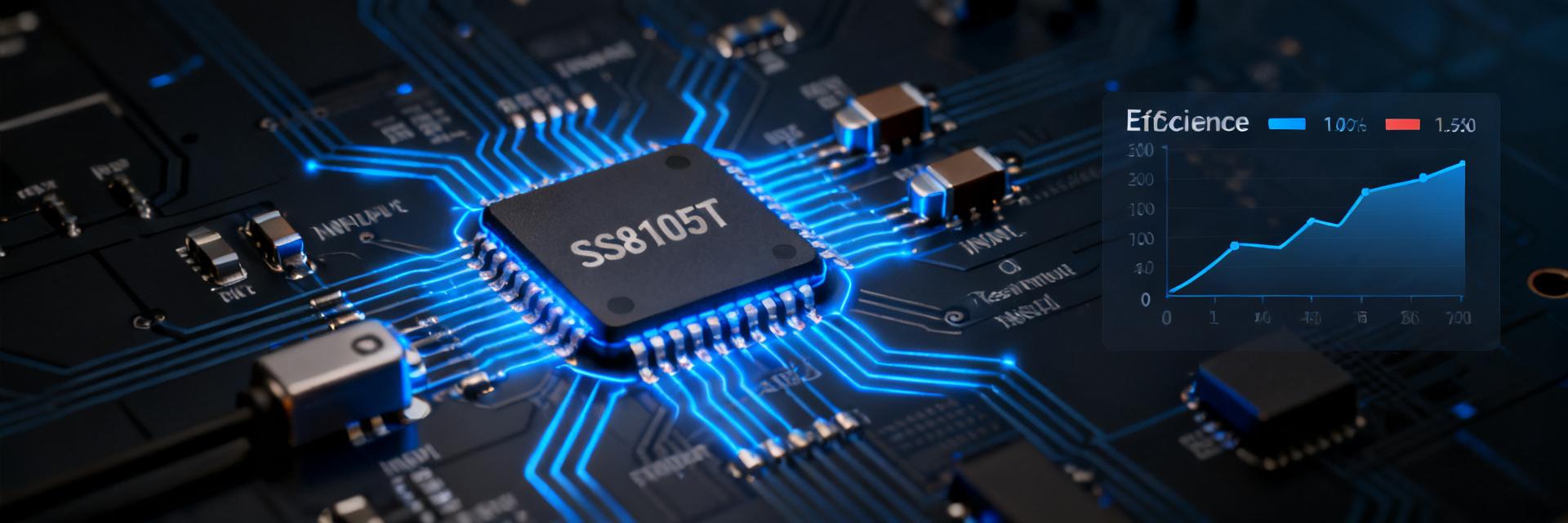
SS8105T adopts an integrated design concept, packaging the high-side and low-side MOSFETs inside a single chip, eliminating the complex selection and drive matching of external power transistors in traditional schemes. Its 15mΩ RDS(on) significantly reduces conduction losses, delivering better temperature rise performance under 4A load conditions compared to discrete solutions.
SS8105T Topology and Integrated MOSFET Characteristics
The chip adopts a synchronous Buck topology with an integrated N-channel MOSFET pair. The high-side MOSFET acts as the main switch, while the low-side MOSFET replaces the freewheeling diode to achieve synchronous rectification. This structure can achieve efficiencies exceeding 93% under heavy loads and automatically switches to pulse-frequency modulation (PFM) / frequency-hopping mode at light loads to maintain high efficiency.
Hysteretic Constant Off-Time Mode vs. Traditional PWM Schemes
Unlike traditional fixed-frequency PWM, the SS8105T employs hysteretic constant off-time control. Under transient load changes, the response speed is improved by 3 to 5 times, and no complex compensation network is required. However, the output ripple is slightly larger than that of voltage-mode schemes, requiring a trade-off between transient performance and ripple metrics.
| Feature / Dimension | Hysteretic Constant Off-Time | Traditional PWM |
|---|---|---|
| Loop Compensation | Not Required | Type II/III |
| Transient Response | Fast (<5μs) | Slower (>20μs) |
| Light-Load Efficiency | Auto Frequency Reduction (PFM) | Forced PWM or Burst Mode |
| EMI Characteristics | Variable Frequency, High Filtering Demand | Fixed Frequency, Highly Predictable |
Pin Definitions and Detailed Functions
A precise understanding of pin functions is essential to avoid soldering rework and functional abnormalities. The SS8105T uses a standard 8-pin package, compatible with both SOP-8 and thermally enhanced ESOP-8 packages.
8-Pin Package (SOP-8/ESOP-8) Pin-by-Pin Mapping Table
| Pin No. | Name | Type | Description |
|---|---|---|---|
| 1 | BST | Power | Bootstrap pin for high-side driver. Connect a 0.1μF ceramic capacitor to SW. |
| 2 | GND | Ground | Power ground. Needs a short and wide connection to the input capacitor ground. |
| 3 | SW | Output | Switch node. Connects to the power inductor. |
| 4 | VIN | Power | Input voltage, range 4.5V to 18V. |
| 5 | EN | Input | Enable control, active high, threshold approx. 1.2V. |
| 6 | COMP | - | Internal compensation node. Leave floating or handle according to the datasheet. |
| 7 | FB | Input | Feedback voltage divider input, reference voltage 0.6V. |
| 8 | SS | - | Soft start control. External capacitor sets the soft-start time. |
Key Pin Design Considerations: BST Bootstrap, EN Enable, FB Divider
The integrity of the BST loop is the lifeline of bootstrap capacitor operation. The capacitor must be placed immediately adjacent to the BST and SW pins, keeping the loop area under 10mm². If the BST voltage is insufficient, the high-side MOSFET will operate in the linear region, leading to catastrophic thermal failure.
The EN pin is compatible with TTL logic and can be directly driven by an MCU GPIO. When designing undervoltage lockout (UVLO), a resistor divider can be connected to EN to implement the input UVLO function, with the hysteresis window determined by the divider ratio.
The accuracy of the FB divider directly determines the output voltage precision. It is recommended to choose 1% tolerance resistors, with the lower resistor (Rlower) on the order of 10kΩ to balance power consumption and noise sensitivity. The output voltage formula is: Vout = 0.6V × (1 + Rupper/Rlower).
Absolute Maximum Ratings and Electrical Characteristics
Exceeding the absolute maximum ratings, even momentarily, can cause potential damage to the device or degrade its lifespan. The design margin should allow for at least a 20% derating headroom.
Voltage/Current/Temperature Stress Boundary Parameters
| Parameter | Symbol | Min | Typ | Max | Unit |
|---|---|---|---|---|---|
| Input Voltage | VIN | 4.5 | 12 | 18 | V |
| Output Current | IOUT | 0 | - | 4 | A |
| Operating Junction Temperature | TJ | -40 | - | 150 | ℃ |
| Storage Temperature | TSTG | -55 | - | 150 | ℃ |
| SW Pin Voltage | VSW | -0.3 | - | VIN+0.3 | V |
Efficiency Curves and Thermal Resistance Data (RθJA/RθJC)
The thermal resistance RθJA of the ESOP-8 package is approximately 45°C/W (standard JEDEC 4-layer board), and RθJC is about 6°C/W. Under 4A full load, 12V to 5V conditions, the estimated junction temperature is: Tj = Ta + (Ploss × RθJA) = 25°C + (0.8W × 45) = 61°C, leaving sufficient margin.
Peak efficiency occurs in the 50% to 70% load range, with typical efficiency reaching 94% for a 12V to 3.3V conversion. In light-load PFM mode, efficiency remains above 80%, which is superior to forced-PWM schemes.
Typical Application Circuits and External Component Calculations
The selection of external components directly determines the upper limit of power supply performance. The integrated features of the SS8105T minimize complexity, but key parameters still require rigorous calculations.
Input Capacitor/Inductor/Output Capacitor Selection Formulas
Input Capacitor: Selected based on the maximum RMS current, Cin ≥ Iout × √(D × (1-D)) / (ΔVin × fsw × 0.8), where D is the duty cycle. It is recommended to parallel a 100μF electrolytic capacitor with a 10μF ceramic capacitor to suppress temperature rise caused by ESR.
Power Inductor: L = (Vout × (Vin - Vout)) / (Vin × ΔIL × fsw). The ripple current ΔIL is typically chosen to be 20% to 40% of the rated current. For 4A applications, 2.2μH to 4.7μH is recommended, and the saturation current must exceed 5.5A.
Output Capacitor: Constrained by both ripple and transient requirements. Ceramic capacitors have extremely low ESR, but their capacitance DC bias derating must be monitored; for electrolytic capacitors, verify that ESR × ΔIL < target ripple.
Loop Stability and Compensation Design Key Points
The hysteretic architecture eliminates external compensation, but the ESR of the output capacitor must meet a minimum requirement to generate sufficient ripple feedback. In all-ceramic output scenarios, a 3-5mΩ resistor can be connected in series, or a version with internal ripple injection can be selected.
Synchronous Buck Converter Selection Decision Framework
The SS8105T is not a universal solution; mapping out its competitive landscape is necessary for precise application matching.
SS8105T vs. Competitor Parameter Comparison Dimensions
| Comparison Item | SS8105T | External MOSFET Schemes | Integrated Competitor A |
|---|---|---|---|
| Integration Level | Integrated Dual MOSFETs | Requires 2 External MOSFETs | Integrated Dual MOSFETs |
| RDS(on) | 15mΩ/15mΩ | Depends on Selection | 25mΩ/25mΩ |
| Switching Frequency | Variable Hysteretic | Fixed/Adjustable | Fixed 1MHz |
| BOM Count | 15-18 pcs | 22-28 pcs | 16-20 pcs |
| Cost Structure | Medium | High (MOS + Driver) | Medium-High |
Scenario-Based Selection: Industrial Power, Consumer Electronics, Battery Powered
Industrial Power Supplies: Prioritize verifying -40°C low-temperature startup and 85°C long-term aging, paying close attention to the SW node ringing amplitude.
Consumer Electronics: Utilize high integration to minimize PCB area, and connect the ESOP-8 thermal pad directly to a large copper plane.
Battery-Powered Applications: Light-load efficiency and quiescent current are core metrics; evaluate no-load losses in PFM/frequency-hopping mode.
Debugging, Troubleshooting, and Empirical Verification
Theoretical design must be verified through empirical closed-loop testing. Common abnormalities have clear troubleshooting paths.
Common Issues: Light-Load Acoustic Noise / Excessive Output Ripple / Thermal Failure
Light-Load Acoustic Noise (Squealing): Typically caused by the switching frequency entering the audible band during PFM mode; this can be suppressed by increasing output capacitance or adjusting the load point.
Excessive Output Ripple: Troubleshoot in three steps—inductor saturation, excessive capacitor ESR, and too large a ground loop area.
Thermal Failure: Locate hot spots using an infrared thermal imager, prioritizing checks on the BST diode reverse recovery and MOSFET conduction losses.
Guide to Capturing Key Waveforms with an Oscilloscope
Four critical waveform sets must be measured: SW node switching waveform (to verify duty cycle and ringing), inductor current triangular wave (to check for saturation), output ripple (AC-coupled, 20MHz bandwidth), and BST-SW bootstrap voltage (to ensure it exceeds the MOSFET threshold).
Key Summary
- Precise Pin Function Control: Among the 8 pins of the SS8105T, BST bootstrap loop integrity, FB divider precision, and EN logic threshold are the three critical design red lines. Any oversight can lead to functional abnormalities or efficiency degradation.
- Strict Electrical Boundary Derating: The 18V maximum input voltage, 4A output current capability, and 150°C junction temperature limit require more than a 20% design margin. For industrial scenarios, it is recommended to keep the junction temperature below 110°C.
- Leverage Hysteretic Architecture Advantages: Eliminating the compensation network accelerates development, but variable switching frequency EMI characteristics must be accepted, and output capacitor selection must balance ESR ripple feedback requirements.
- Do Not Neglect Thermal Design: The ESOP-8 package features an RθJA of approx. 45°C/W. Under a 4A full-load scenario, it is critical to ensure that the thermal pad effectively conducts heat to the PCB copper plane.
- Key Verification Points for Competitor Replacement: When migrating from external MOSFET schemes, focus on comparing transient response speeds and light-load efficiency curves to prevent loop instability caused by direct pin-to-pin replacements.
FAQ
How to select the FB pin voltage divider resistors for the SS8105T synchronous buck converter to ensure output voltage accuracy?
It is recommended to use a 10kΩ resistor for the lower divider resistor, and calculate the upper divider resistor using Vout = 0.6V × (1 + Rupper/Rlower). Select 1% tolerance resistors with a temperature coefficient (tempco) of ≤100ppm/°C. During layout, keep the FB trace away from the SW switching node, and if necessary, place a 10pF-47pF filter capacitor close to the FB pin to suppress noise coupling.
Can the SS8105T directly replace external Schottky diodes in traditional asynchronous buck schemes?
Yes, and the efficiency improvement is significant. The SS8105T integrates a low-side MOSFET to replace the Schottky diode, eliminating diode forward voltage drop losses. When replacing, the inductor value needs to be recalculated (as the original scheme was designed based on asynchronous ripple) and the PCB copper area should be verified to meet the heat dissipation requirements for the slightly higher switching noise of the synchronous scheme.
How can the light-load efficiency of the SS8105T be optimized in battery-powered scenarios?
The chip automatically enters frequency-hopping (PFM) mode to reduce switching losses. To optimize further, you can increase the inductor value to reduce ripple current, select a low-DCR inductor, and use X5R/X7R ceramic capacitors for all output capacitors to minimize leakage current. System-level optimization can incorporate EN shutdown control to reduce shutdown quiescent current to the μA level.
How to troubleshoot frequent failures of the BST bootstrap capacitor on the SS8105T?
The root cause of failure is usually insufficient capacitor voltage rating or excessive loop inductance. A X5R/X7R ceramic capacitor with a voltage rating of ≥16V and a capacitance of 0.1μF must be used, placed tightly adjacent to the BST and SW pins. Measure the BST-SW voltage with an oscilloscope; it should normally remain at 4.5V-5.5V. If a drop occurs, check the capacitor ESR or add a parallel capacitor.
How to quickly assess if heat dissipation is sufficient when selecting the SS8105T synchronous buck converter?
Simple estimation: Ploss = Iout² × (Rds(on)_hs × D + Rds(on)_ls × (1-D)) + Switching Loss, Tj = Ta + Ploss × RθJA. If Tj > 110°C, prioritize switching to the ESOP-8 package for enhanced thermal dissipation, or reduce the switching frequency, increase the copper plane area, and introduce thermal vias to conduct heat to the inner layers.